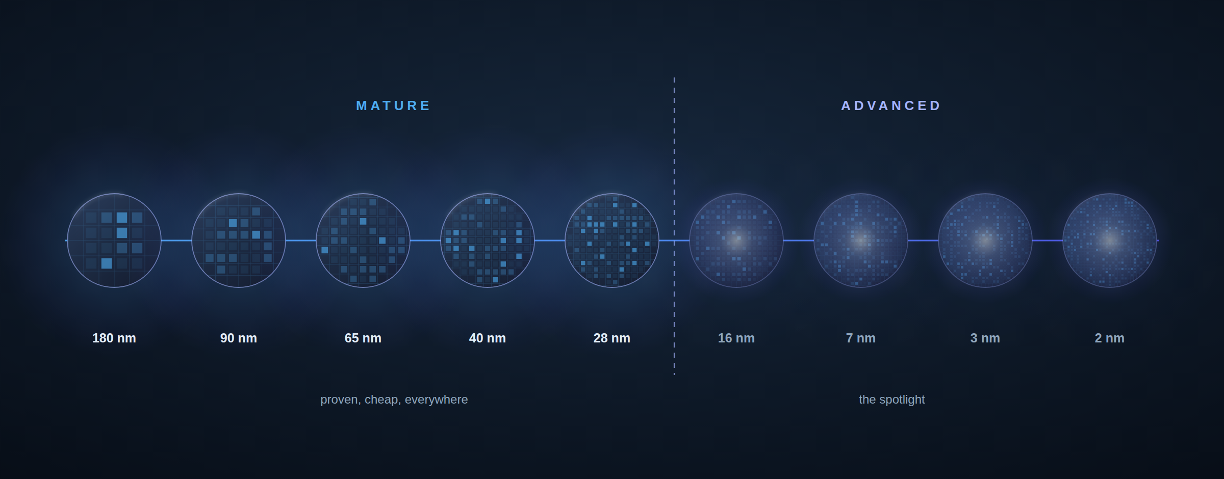
In semiconductor manufacturing, a mature node is an established process generation behind the technological leading edge, commonly but not universally defined as 28 nm or larger. These processes are characterized by stable yields, deep design ecosystems, and long production histories. Their equipment is often, though not necessarily, largely written down. By capacity, most foundry output runs on them: TrendForce projected a roughly 70:30 mature-to-advanced split holding from 2023 through 2027.[1]
Depreciation is a common characteristic of mature-node production, not part of the definition. Some mature fabs run substantially written-down tools; others run upgraded or newly installed equipment on the same process generation. The definition rests on process generation, stability, and established volume production, not on accounting status.
Where the boundary is drawn
There is no single authority for the term, and the bodies that use it in binding documents do not agree on one threshold. Most place the line at or around 28 nm, some at 40 nm, and the regulatory definitions carry additional criteria that a single nanometer figure does not capture. The table below is an orientation, not a substitute for the source documents, which govern.
| Source | Boundary | Term used |
|---|---|---|
| US CHIPS Act guardrails and Commerce regulations | Varies by category. Distinct treatment for logic, memory, analog and other classes, with further criteria covering wafer size and packaging. Frequently summarized as 28 nm and older for logic, but that summary is not the whole rule. | Legacy semiconductor[2] |
| US Trade Representative, Section 301 | States no nanometer threshold. Treats the category as also known as legacy or mature-node, and weighs incorporation into downstream products in critical industries. The investigation concluded in December 2025 with an affirmative determination; the added tariff starts at 0 percent and rises in June 2027. | Foundational semiconductor[3] |
| Market research and industry usage | At or above roughly 28 nm | Mature node[1] |
| Common looser usage | 40 nm and above | Legacy node |
The practical effect is that a claim about mature-node capacity can shift substantially depending on whose definition is in use, which matters most in trade filings and capacity forecasts. When a figure is cited without its threshold, the threshold is worth asking for.
The other names for it
- Legacy node
- The most common synonym, and the term used in US statute and regulation. It carries an implication of obsolescence that the economics do not support, since these processes are in current volume production.
- Trailing-edge node
- The neutral counterpart to leading-edge. Common in trade and policy writing where “legacy” would prejudge the question.
- Foundational semiconductor
- The US Trade Representative’s term, which it treats as interchangeable with legacy and mature-node while emphasizing what depends on the part.[3]
- Workhorse node
- Informal, descriptive industry language rather than a defined term. Most often applied to 28 nm, reflecting its long run as a cost-effective general-purpose logic process, though it is not a formal synonym and is used loosely.
- Mainstream node
- Occasionally used for the band immediately behind the leading edge, which is neither frontier nor fully mature.
Why the line sits near 28 nanometers
TSMC brought its 28 nm foundry process to volume production in 2011, and mainstream foundry adoption of FinFET transistors followed at 16 and 14 nm. That makes 28 nm the last generation at which planar transistors were the mainstream foundry choice, which is one reason the boundary is drawn near it. The picture is not perfectly clean: transistor architectures differ between manufacturers, TSMC’s intermediate 20 nm process was also planar, and FD-SOI processes at 22 nm and below remain planar today.
The economic argument carries more weight. An influential industry finding holds that conventional cost-per-transistor scaling stalled around 28 nm. Each earlier generation had delivered smaller transistors that were also cheaper, which is the compounding that made Moore’s Law an economic law and not merely a physical one; from roughly 28 nm forward that relationship weakened. The observation was published by Zvi Or-Bach in 2014 and restated by Google’s Milind Shah at IEDM in 2023.[4] It is a widely cited finding rather than a universal law: realised cost per transistor varies with chip design, foundry, yield, density assumptions and production volume, and some large-die products have continued to see modest declines.
The practical consequence is clearer. Below 28 nm a designer is buying density, speed, and power efficiency, and paying substantially higher mask and design costs to get them. For a product that needs those things, the trade is worth making. For a product that does not, moving down a node may raise total cost without delivering a useful product-level benefit.
What is built on mature nodes
Mature nodes carry much of the semiconductor content that is not a processor. Analog and mixed-signal parts, power management ICs, microcontrollers, and many display drivers are predominantly built on mature logic processes.
Several other categories are commonly grouped under the same heading but do not map cleanly onto logic-node nanometer labels at all. Image sensors, RF front ends, MEMS devices, and discrete power components such as power MOSFETs, IGBTs and silicon-carbide devices are made on specialized processes described by their own parameters rather than by a logic node. They belong to the same economic story and not to the same measuring system.
- Legacy chips accounted for roughly 95 percent of the automotive industry’s semiconductor consumption, as of a 2023 assessment. The same assessment puts the chip count of an average vehicle at around 1,700, though counts of this kind vary widely with vehicle type and with what is counted as a chip.[5]
- The industry shipped a record 1.15 trillion semiconductor units in 2021. No authoritative breakdown of those units by process node exists, but the categories that dominate unit volume, analog, power, microcontroller, sensor and connectivity parts, are largely mature-node products.[6]
- AI datacenters depend on them by chip count. The power ICs and other support devices in most GPU systems are built on nodes far larger than the processors they supply, though integration and process choices vary by design.
The automotive shortage that began in 2021 is the clearest demonstration of the dependency. The parts that halted vehicle assembly were microcontrollers and analog and power devices on processes a decade or more old, not the leading-edge logic that dominated coverage of the same period. AlixPartners forecast the cost to the global auto industry at $210 billion of 2021 revenue and 7.7 million vehicles of lost production.[7]
One distinction is worth keeping straight, because it is where most writing on the subject goes wrong. Mature nodes carry the physical economy, meaning capacity, unit volume, and the downstream products that cannot ship without them. The leading edge captures the industry’s revenue and profit premium. A claim that mature nodes are most of the industry is often true by capacity or unit volume, but generally not by revenue, and the two measures get swapped freely.
Why mature nodes are not retired
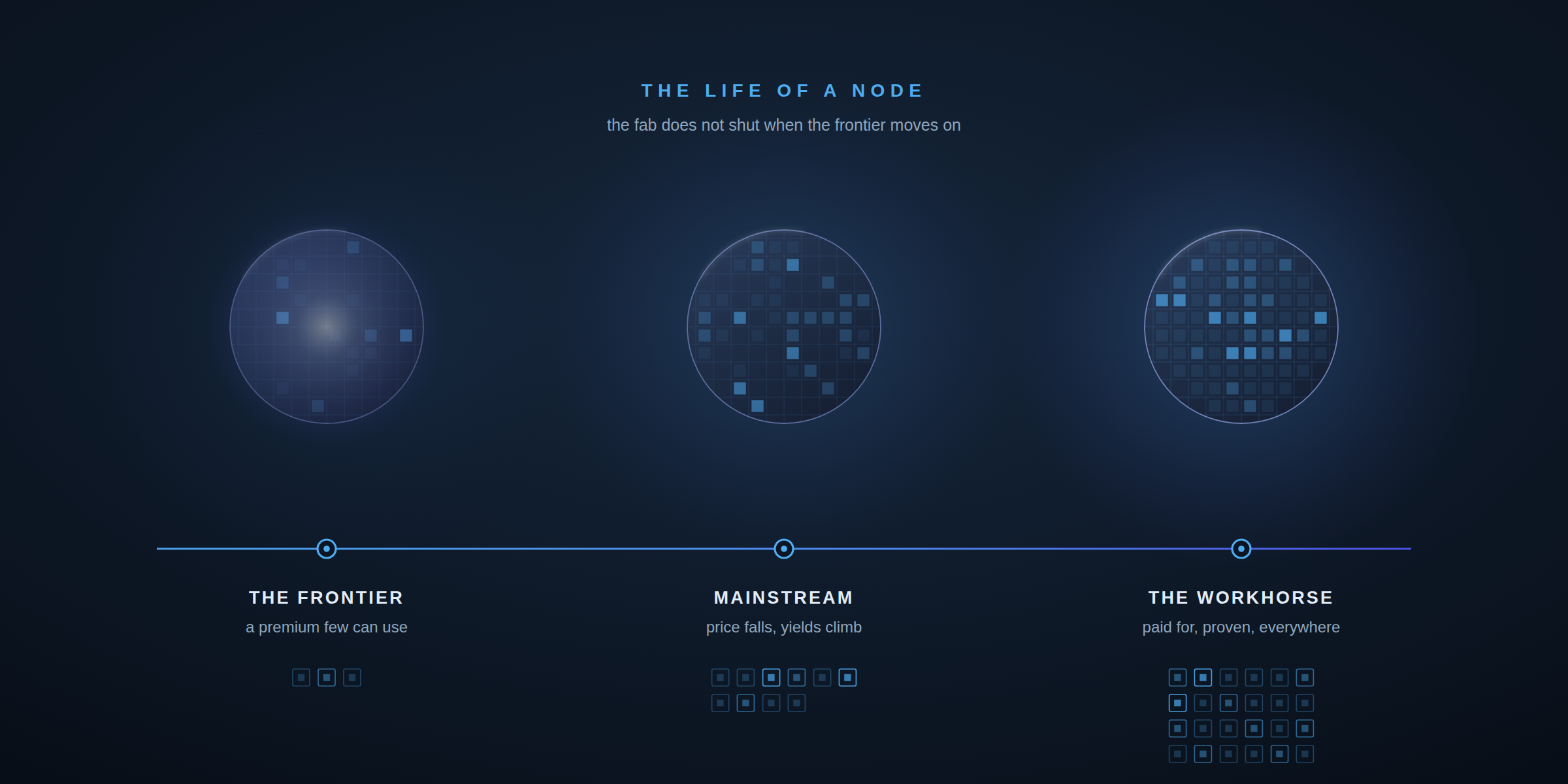
A fab does not close when the frontier moves past it. Four things keep mature capacity in production.
- The equipment is largely written down. Fab machinery is depreciated over a handful of years and buildings over a couple of decades.[8] A process that outlives its equipment’s book life carries a lower capital cost base than a new fab can match. That is a real advantage and not a free ride: mature fabs still carry maintenance, refurbishment, consumables, labor, and periodic capital upgrades.
- The process is debugged. Yield on a node that has run for years across large wafer volumes is high and predictable, and the design ecosystem around it is deep: mature IP libraries, established tooling, shorter design cycles, and cheaper mask sets.
- Qualification is expensive to repeat. Automotive, industrial, medical, and defense parts are qualified against standards that assume long production lifetimes. Moving a qualified part to a new process means requalifying it, which routinely costs more than the die savings return.
- Analog, power, and RF do not shrink well. Digital logic gets faster and cheaper as it gets smaller. Precision analog does not, because matched devices need physical area to match accurately, and power devices need area and thicker oxides to handle current and voltage. Shrinking these parts degrades them, so they stay on the processes that suit them.
Node names are not measurements
The nanometer figure in a node name has not described a physical feature for a long time. Early process names tracked a real dimension, typically transistor gate length or metal half-pitch. As scaling continued, the naming detached from any single measurable feature and became a commercial designation for a generation of process technology.
Two consequences follow. Identically named nodes from different foundries are not equivalent, and differ in transistor density, performance, and power. And a boundary defined as 28 nm and above is a line drawn across names rather than physics, which is part of why the definitions above vary and why regulators pair the node figure with wafer size and packaging criteria.
References
- TrendForce, “China’s Share in Mature Process Capacity Predicted to Hit 29% in 2023, Climbing to 33% by 2027” (October 2023), which projects the global mature-to-advanced ratio at about 7:3 across 2023–2027 and treats mature as at or above roughly 28 nm. trendforce.com
- US CHIPS and Science Act guardrail provisions and the US Department of Commerce implementing regulations. These set out category-specific treatment for logic, memory, analog and other semiconductor classes, together with criteria covering wafer size and packaging. The regulation text is the operative definition and should be read directly; the summary in the table above is an orientation.
- Office of the United States Trade Representative, Section 301 investigation into China’s acts, policies, and practices related to targeting of the semiconductor industry for dominance (initiated December 2024; affirmative determination and Notice of Action 23 December 2025, with an added tariff set at 0 percent and scheduled to rise on 23 June 2027), which uses “foundational semiconductors,” describes them as also known as legacy or mature-node semiconductors, and addresses their incorporation into downstream products in critical industries. Congressional Research Service, “Section 301 and China: Mature-Node Semiconductors” (IF12958).
- Zvi Or-Bach, “28nm: The Last Node of Moore’s Law,” EE Times (2014); Milind Shah (Google) at IEDM 2023, reporting that transistor cost scaling stalled at 28 nm and has remained flat generation over generation since. Both are influential industry analyses rather than settled measurement, and reported cost per transistor varies with design, foundry, yield and volume.
- Center for Strategic and International Studies, “The Strategic Importance of Legacy Chips” (2023). csis.org Per-vehicle chip counts are estimates and vary considerably by vehicle type and counting method; other published figures range from roughly 1,400 to 3,000.
- Semiconductor Industry Association, 2021 unit shipments (February 2022): a record 1.15 trillion units. The SIA figure is a unit total and does not include a breakdown by process node.
- AlixPartners forecast (September 2021): $210 billion in lost 2021 global automotive revenue and 7.7 million vehicles of lost production. Node attribution for the bottleneck parts: SemiEngineering, “Chip Shortages Grow For Mature Nodes” (2021). semiengineering.com
- TSMC Form 20-F (US Securities and Exchange Commission): machinery and equipment depreciated straight-line over 5 years, buildings over 10 to 20 years (2025 report, filed April 2026). Depreciation schedules are an accounting measure and do not describe a fab’s operating costs.
Last reviewed 20 October 2026. Figures are dated in the text; where a source has published newer data, the source governs.